Inverse design of grating coupler on SOI for angled fiber. (inverse design not available in free version)
Config
import os
import numpy as np
import matplotlib.pyplot as plt

import gdsfactory as gf
from gdsfactory.technology import LogicalLayer, LayerLevel, LayerStack
import luminescent as lumi

path = os.path.join("runs", "GC_invd")

wl = 1.55
bandwidth = 0.01
nwls = 3
wls = np.linspace(wl - bandwidth / 2, wl + bandwidth / 2, nwls)

# simulation parameters
nres = 6
boundaries = ["PML", ["PEC", "PML"], "PML"]
PML_decay = [0.01, 0.3, 0.01]
courant = 0.95
# stop_decay=.001
stop_decay=None

# horizontal dimensions
D = 10.4  # mode field diameter, SMF-28
R =  D  # beam frame
flare = 25  # waveguide flare full angle (deg)
W = 3 * D
# L = W
L = W/2/np.tan(flare/2/180*np.pi)
w_wg = 0.5
l_wg =1
l_flare = .5

margin = .5
nox=1.44
# vertical dimensions
theta = 7 * np.pi / 180 # beam angle
h_wg = 0.22
h_etch = 0.08
h_slab = h_wg-h_etch
# h_box = 2.0  # buried oxide
h_box = (1 + .5) *wl / (2 * nox * np.cos( theta))
h_sub = 0.3  # substrate thickness in domain

zmargin = .6
port_offset = 0.3
source_offset = 0.3
z_port = h_wg + port_offset

zmin = -h_box - h_sub
zmax = h_wg + port_offset + source_offset

# movie parameters
shot_every = 10

views = [
    lumi.view("Ey", y=0, z=h_slab+h_etch/2,mirrors = ["y-"]),
]

# materials
core = "Si"
clad = "SiO2"
materials = {
    "Si": lumi.material(3.45),
    "SiO2": lumi.material(1.44),
}

n_core = materials[core]["n"]
n_clad = materials[clad]["n"]
lambda_core = wl / n_core
lambda_clad = wl / n_clad
dx = lambda_core / nres

background = clad
materials["design"] = lumi.placeholder_material(n_core)

# layer stack. lower mesh order layers override higher mesh order layers.
WG = (1, 0)
CLAD = (2, 0)
SLAB = (102, 0)
DESIGN = (1001, 0)
CONTOUR=(1002,0)

layers = {
    "design": LayerLevel(
        layer=LogicalLayer(layer=DESIGN),
        zmin=h_slab,
        thickness=h_etch,
        material="design",
        mesh_order=1,
    ),
    "rib": LayerLevel(
        layer=LogicalLayer(layer=SLAB),
        zmin=h_slab,
        thickness=h_etch,
        material=core,
        mesh_order=101,
    ),
    "slab": LayerLevel(
        layer=LogicalLayer(layer=SLAB),
        zmin=0,
        thickness=h_slab,
        material=core,
        mesh_order=102,
    ),
    "core": LayerLevel(
        layer=LogicalLayer(layer=WG),
        zmin=0,
        thickness=h_wg,
        material=core,
        mesh_order=200,
    ),
    "substrate": LayerLevel(
        layer=LogicalLayer(layer=CLAD),
        zmin=zmin,
        thickness=h_sub,
        material=core,
        mesh_order=300,
    ),
}
layer_stack = LayerStack(layers=layers)

optimizer = lumi.optimizer(
    stoploss=0.3,
    lowloss=0.5,
    iters=20,
    contrast=0.5,
    momentum=0.7,
)
targets = [
    lumi.target(src="o2@0-", dst="o1@0+", target=1, weight=1 / nwls, wl=wl)
    for wl in wls
]
lmin=.1
lumi backend: None
Geometry
# Build the gdsfactory component to be optimized (upper half, mirrored about y=0).
x_design = -L + R
# x_flare = ox_design - l_flare
# x_wg = x_flare - l_wg

c = gf.Component()
for layer in (DESIGN, ):
    rect = c << gf.components.rectangle(size=(L, W / 2), layer=layer)
    rect.movex(x_design)

# w_flare = w_wg / 2 + l_flare * np.tan(np.radians(flare / 2))
x_wg=x_design-l_wg
p=[(x_design,0),(x_design,w_wg/2),(x_design+L,W/2),(x_design+L,0)]
c.add_polygon([(x_wg, 0), (x_wg, w_wg / 2), (x_design, w_wg / 2), (x_design,0)], layer=WG)
c.add_polygon(p, layer=CONTOUR)
c.add_polygon(p, layer=SLAB)

c << gf.components.bbox(component=c, layer=CLAD, top=margin, right=margin)

c.add_port("o1", center=(x_wg, 0), width=w_wg / 2, orientation=180, layer=WG)


c.plot()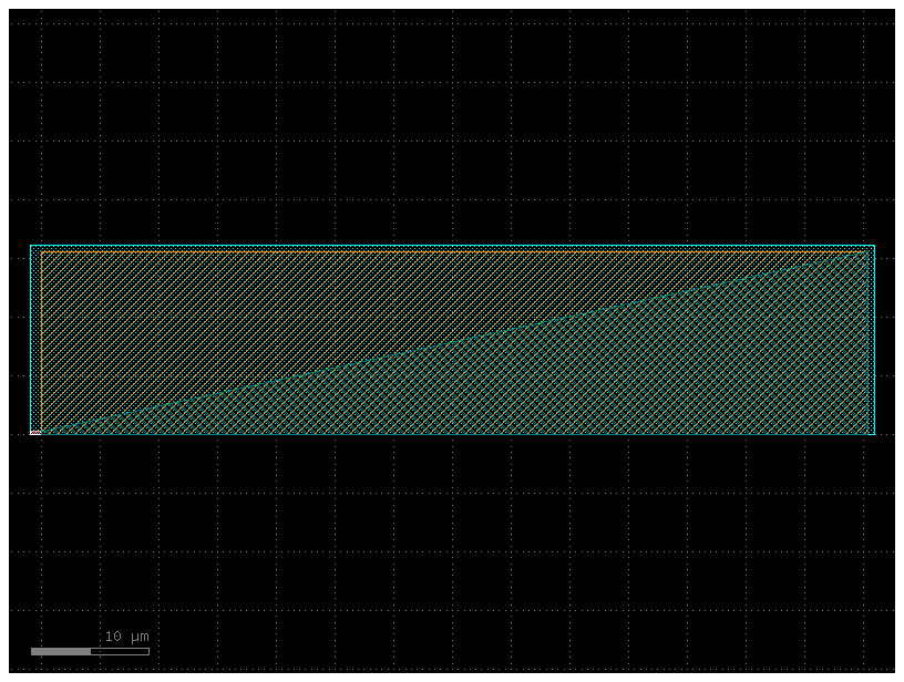
frames = [
    lumi.plane_frame(
        "wg",
        start=[-w_wg / 2 - margin, -zmargin],
        stop=[0, h_wg+zmargin],
        boundaries=[("PML", "PEC"), "PML"],
        wls_mode_solver=[wl],
    ),
    lumi.plane_frame(
        "beam",
        modes=[
            [
                lumi.gaussian_mode(
                    D,
                    n_clad,
                    dx=dx,
                    theta=theta,
                    wl=wl,
                    half="y+",
                    Dlim=2*R,
                )
            ]
        ],
        start=[-R, 0],
        stop=[R, R],
    ),
]

origin = [
    np.sin(theta) * (source_offset + port_offset),
    0,
    h_wg + port_offset + source_offset,
]
basis = [[1, 0, 0], [0, 1, 0], [0, 0, 1]]
sources = [
    lumi.source(
        "o2",
        origin,
        basis,
        wl=wl,
        bandwidth=max(max(wls) - min(wls), wl / 4),
        frame="beam",
    )
]

origin = [np.sin(theta) * (port_offset), 0, h_wg + port_offset]
monitors = [
    lumi.gf_monitor("o1", c, layer_stack, frame="wg"),
    lumi.monitor("o2", origin, basis, frame="beam"),
]


designs = [
    lumi.design(
        name="design",
        lmin =lmin,
        layer=DESIGN,
        contour_layer=CONTOUR,
        fill_material=core,
        void_material=clad,
        component=c,
        layer_stack=layer_stack,
        materials=materials,
        repdims=[3],
        anchordims=[],
    )
]

tmax =     1.2/ wl    * (
        (port_offset + source_offset + 2 * h_box) / np.cos(theta) * n_clad
        + (L + W / 2 + R + l_wg) * n_core
    )    + sources[0]["duration"]

bbox = c.bbox_np().tolist()
bbox[0].append(zmin)
bbox[1].append(zmax)Solve
lumi.mesh(path, c, layer_stack, materials, zmin, zmax)
lumi.setup(
    path=path,
    wl=wl,
    wls=wls,
    frames=frames,
    monitors=monitors,
    sources=sources,
    boundaries=boundaries,
    bbox=bbox,
    materials=materials,
    background=background,
    nres=nres,
    tmax=tmax,
    PML_decay=PML_decay,
    courant=courant,
    stop_decay=stop_decay,
    shot_every=shot_every,
    views=views,
    designs=designs,
    targets=targets,
    optimizer=optimizer,
    # load_designs=['design']
)
Warning: boolean difference failed at index 1: Difference only defined over two meshes.
showing modes for wavelength 1.55
mode Boundary conditions: 00A0
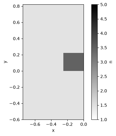
wg/1.55 mode 0 (neff=2.409+0.000j)
saving mode to runs/GC_invd/modes/wg/1.55/0.npz
using simulation folder runs/GC_invd
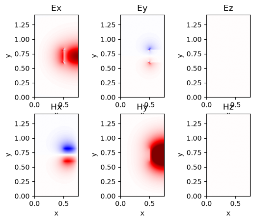
Movie
lumi.movie(path)Loading...